When you are talking about electronics and circuit design, two terms come up: PCB design and VLSI design. While both are vital components in the creation of modern electronic devices, they refer to different aspects of the process. Understanding the differences between these two fields is crucial for engineers and designers who work in the electronics industry, as they involve distinct approaches, tools, and skill sets.
Let’s dive into the details of each, exploring what they involve and how they differ from each other
What is PCB Design?
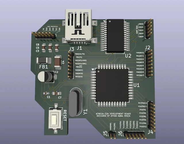
PCB (printed circuit board) design refers to the process of designing the physical layout of a circuit board that connects and supports various electronic components such as resistors, capacitors, and ICs (integrated circuits). Essentially, a PCB serves as the backbone of many electronic devices, providing the electrical connections between components
PCB design involves several stages
Schematic Design: Engineering first creates schematics that are complete, engineers choose the appropriate components that determine the flow of electricity within the board and rotation, and ICS work together effectively.
Layout Design: This is the actual design of the physical PCB. Engineers use PCB design software (Like Eagle, Altium Designer, or Kicad) to create the layout. This spet involves placing the components on the board and routing electrical traces to connect them.
Simulation and Testing:Once the design passes simulations, the manufacturer fabricates and assembles the PCB.
Key Features of PCB Design:
- Physical design: focused on the layout, the arrangement of components, and rotating of electrical traces on the board.
- Electronics connectivity: ensure the components communicate with each other properly.
- Manufacturing Process: The design is ready to be sent to manufacturers who will create the physical board.
- Design Software: Engineers rely heavily on specialized PCB design tools for creating layouts, checking for design rule violations, and managing component libraries.
What is VLSI Design?
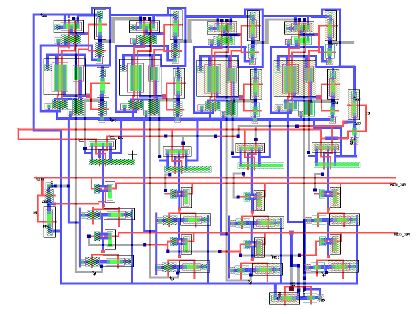
VLSI (Very Large Integrations) refers to the process of designing integrated circuits (ICS) that contain thousands, millions, or even billions of transistors on a single chip.
VLSI design is highly complex and typically involves the following stages:
- Specification: the initial stage involves understanding the functional requirements of the integrated circuits, such as the types of operations it will perform or the data it will process.
- RTL:Engineers translate high-level designs into low-level representations by describing the data flow between registers, which is then used to create hardware.
- Logic Design: engineering designs the logic circuits that will perform the options described in the specifications. This includes defining gates, flip-flops, multiplexers, and logical elements.
- Physical design: the physical design stage is where the layout of the transistor is created on the silicon chip. This is similar to the PCB layout but on a microscopic level. Transistors, metal layers, and connections are arranged carefully to meet the timing and power requirements
- Testing: after fabrication, the ICs undergo rigorous testing to ensure they meet design specifications. this includes functional testing and timing analysis. AMD power consumption checks,
- Fabrication: After the design is verified, it is sent to a semiconductor foundry where the IC is fabricated using photolithography and other processes.
Key Features of VLSI Design:
- Microchip Design: Creating chips with millions/billions of transistors
- .High Complexity: Requires precise planning to ensure functionality
- .Advanced Tools: Uses CAD, simulation software, and HDLs like Verilog/VHDL.
Key Differences Between PCB Design and VLSI Design
While both PCB and VLSI design play significant roles in electronics, there are several fundamental differences between the two fields:
- Scale and scope:
- PCB design involves designing physical boards that connect and support electronic components
- VLSI design involves designing a very complex integrated circus with millions or billions of transistors packed into a tiny chip.
- Nature of work
- PCB designers are concerned with what layout of the components and the routing of electrical connections on a board.
- VLSI designers focus on creating tiny electronic circuits with numerous transistors that can perform highly complex operations in minimal physical space.
- Level of Abstraction:
- PCB design is a relatively lower-lave;l design compared to VLSI, focusing more on the physical layout and electrical connections.
- VLSI design operates at a higher level of abstraction, dealing with logic gates, flip-flops, and data flow before translating these designs into physical translators
- Toolset
- PCB designers use CPB design tools like Altuyum Designers, KiCad, or Eagle m which are tailored to crating board layouts.
- VSLI designer: use specialized tools for logic Degner, simulation, and verifications, such as cadence, Synopsys, and tools for writing
Conclusion
In summary, PCB (Printed Circuit Board) design and VLSI (Very Large Scale Integration) design serve distinct purposes in the electronics industry. PCB design focuses on creating the physical layout of circuit boards, and connecting various electronic components to ensure proper functionality. On the other hand, VLSI design involves integrating millions to billions of transistors onto a single chip, enabling high-performance computing and miniaturized electronic devices.
While PCB design is essential for assembling electronic systems, VLSI is at the core of advanced semiconductor technology. Both fields play a critical role in modern electronics, working together to power everything from everyday gadgets to complex computing systems. Understanding their differences helps engineers choose the right approach for their specific design needs.